PWM i ADC
U ovom poglavlju ćemo se baviti ADC-om i hardverskim high resolution PWM izlazom. Iskoristićemo već postojeći projekat "ADC - SimpleDACtoADC" koji se nalazi u direktorijumu "C:\ti\controlSUITE\development_kits\Piccolo controlSTICK\ADC - SimpleDACtoADC". Projekat je potrebno uvući u razvojno okruženje na isti način kako je to rađeno sa projektom iz prethodnog poglavlja.
Glavni program treba da izgleda kao na listingu. Ako to nije slučaj, potrebno je kod sa listinga iskopirati u datoteku "SimpleDACtoADC - Main.c".
//------------------------------------------------------------------------------------
//    FILE:            SimpleDACtoADC-Main.c
//
//    Description:    This program demonstrates continuous ADC conversion of one channel
//                    where a filtered PWM (DAC) output using ePWM1A is used as the
//                    input signal. Edit the "duty_cycle" variable to modify the DAC
//                    output voltage level and view the variable adc_result to view the
//                    value sampled by the ADC.
//
//                    ***The user should connect PWM-DAC (pin31) to ADC0 (pin3)***
//
//  Target:          TMS320F2802x or TMS320F2803x families (Piccolo)
//
//------------------------------------------------------------------------------------
//  $TI Release:$     V1.1
//  $Release Date:$ 26 Oct 2009 - BL
//------------------------------------------------------------------------------------
//
// PLEASE READ - Useful notes about this Project

// Although this project is made up of several files, the most important ones are:
//        - "SimpleDACtoADC.c",    this file
//        - Application Initialization, Peripheral config
//        - Application management
//        - Slower background code loops and Task scheduling
//     "SimpleDACtoADC-DevInit_F28xxx.c"
//        - Device Initialization, e.g. Clock, PLL, WD, GPIO mapping
//        - Peripheral clock enables
// The other files are generally used for support and defining the registers as C
// structs. In general these files will not need to be changed.
//   "F28027_RAM_SimpleDACtoADC.CMD" or "F28027_FLASH_SimpleDACtoADC.CMD"
//        - Allocates the program and data spaces into the device's memory map.
//   "DSP2802x_Headers_nonBIOS.cmd" and "DSP2802x_GlobalVariableDefs.c"
//        - Allocate the register structs into data memory.  These register structs are
//          defined in the peripheral header includes (DSP2802x_Adc.h, ...)
//
//----------------------------------------------------------------------------------

#include "PeripheralHeaderIncludes.h"
#include "DSP2802x_EPwm_defines.h"         // useful defines for initialization


//%%%%%%%%%%%%%%%%%%%%%%%%%%%%%%%%%%%%%%%%%%%%%%%%%%%%%%%%%%%%%%%%%%%%%%%%%%%%%%%%%%
// FUNCTION PROTOTYPES
//%%%%%%%%%%%%%%%%%%%%%%%%%%%%%%%%%%%%%%%%%%%%%%%%%%%%%%%%%%%%%%%%%%%%%%%%%%%%%%%%%%

void DeviceInit(void);
void InitFlash();
void MemCopy(Uint16 *SourceAddr, Uint16* SourceEndAddr, Uint16* DestAddr);

//%%%%%%%%%%%%%%%%%%%%%%%%%%%%%%%%%%%%%%%%%%%%%%%%%%%%%%%%%%%%%%%%%%%%%%%%%%%%%%%%%%
// VARIABLE DECLARATIONS - GENERAL
//%%%%%%%%%%%%%%%%%%%%%%%%%%%%%%%%%%%%%%%%%%%%%%%%%%%%%%%%%%%%%%%%%%%%%%%%%%%%%%%%%%

// Used for running BackGround in flash and the ISR in RAM
extern Uint16 RamfuncsLoadStart, RamfuncsLoadEnd, RamfuncsRunStart;
Uint16 adc_result;
Uint16 duty_cycle;


//%%%%%%%%%%%%%%%%%%%%%%%%%%%%%%%%%%%%%%%%%%%%%%%%%%%%%%%%%%%%%%%%%%%%%%%%%%%%%%%%%%
// MAIN CODE - starts here
//%%%%%%%%%%%%%%%%%%%%%%%%%%%%%%%%%%%%%%%%%%%%%%%%%%%%%%%%%%%%%%%%%%%%%%%%%%%%%%%%%%
void main(void)
{
    Uint16 i = 0;

//=================================
//    INITIALISATION - General
//=================================

    DeviceInit();    // Device Life support & GPIO mux settings

// Only used if running from FLASH
// Note that the variable FLASH is defined by the compiler (-d FLASH)
#ifdef FLASH
// Copy time critical code and Flash setup code to RAM
// The  RamfuncsLoadStart, RamfuncsLoadEnd, and RamfuncsRunStart
// symbols are created by the linker. Refer to the linker files.
    MemCopy(&RamfuncsLoadStart, &RamfuncsLoadEnd, &RamfuncsRunStart);

// Call Flash Initialization to setup flash waitstates
// This function must reside in RAM
    InitFlash();    // Call the flash wrapper init function
#endif //(FLASH)


//===============================================================
// PWM INITIALISATION to use pin31(PWM1A-DAC) as ADC input source
//===============================================================
#define period 30                           // 2MHz when PLL is set to 0xC (60MHz)
                                           // 60MHz / 30 = 2MHz

    duty_cycle = 15;                       // Initialize to 50% duty cycle

  // Time-base registers
    EPwm1Regs.TBPRD = period;              // Set timer period, PWM frequency = 1 / period
    EPwm1Regs.TBPHS.all = 0;               // Time-Base Phase Register
    EPwm1Regs.TBCTR = 0;                       // Time-Base Counter Register
    EPwm1Regs.TBCTL.bit.PRDLD = TB_IMMEDIATE;  // Set Immediate load
    EPwm1Regs.TBCTL.bit.CTRMODE = TB_COUNT_UP; // Count-up mode: used for asymmetric PWM
    EPwm1Regs.TBCTL.bit.PHSEN = TB_DISABLE;       // Disable phase loading
    EPwm1Regs.TBCTL.bit.SYNCOSEL = TB_SYNC_DISABLE;
    EPwm1Regs.TBCTL.bit.HSPCLKDIV = TB_DIV1;
    EPwm1Regs.TBCTL.bit.CLKDIV = TB_DIV1;

    // Setup shadow register load on ZERO
    EPwm1Regs.CMPCTL.bit.SHDWAMODE = CC_SHADOW;
    EPwm1Regs.CMPCTL.bit.LOADAMODE = CC_CTR_ZERO; // Load on CTR=Zero

    // Set compare values
    EPwm1Regs.CMPA.half.CMPA = duty_cycle;          // Set duty 50% initially

    // Set actions
    EPwm1Regs.AQCTLA.bit.ZRO = AQ_SET;            // Set PWM1A on Zero event
    EPwm1Regs.AQCTLA.bit.CAU = AQ_CLEAR;          // Clear PWM1A on Up-Count CompareA event

//=======================
// ADC INITIALISATION
//=======================

    EALLOW;
    AdcRegs.ADCCTL1.bit.ADCREFSEL   = 0;     // use internal band gap reference
    AdcRegs.ADCCTL1.bit.ADCBGPWD    = 1;     // power up band gap
    AdcRegs.ADCCTL1.bit.ADCREFPWD   = 1;     // power up reference
    AdcRegs.ADCCTL1.bit.ADCPWDN     = 1;     // power up rest of ADC
    AdcRegs.ADCCTL1.bit.ADCENABLE   = 1;     // enable ADC output
    for(i=0; i<5000; i++){}                  // wait 60000 cycles = 1ms (each iteration is 12 cycles)

    AdcRegs.ADCCTL1.bit.INTPULSEPOS    = 1;  // create int pulses 1 cycle prior to output latch

    //EOC = end of conversion event, SOC = start of conversion event
    AdcRegs.INTSEL1N2.bit.INT1SEL = 0;        // ADCCH0 (ADC-A0) EOC causes ADCInterrupt1
    AdcRegs.INTSEL1N2.bit.INT1CONT = 1;        // set ADCInterrupt 1 to auto clr (continuous conversion)
    AdcRegs.INTSEL1N2.bit.INT1E = 1;        // enable ADCInterrupt1; 0=none, 1=ADCInt1, 2=ADCInt2

    AdcRegs.ADCINTSOCSEL1.bit.SOC0 = 1;        // ADCInterrupt1 causes SOC0
    AdcRegs.ADCSOC0CTL.bit.CHSEL= 0;         // convert ADC-A0 (CH0) when SOC0 is received
    AdcRegs.ADCSOC0CTL.bit.ACQPS = 6;        // set S/H window to 6 clk cycles (117ns)

    AdcRegs.ADCSOCFRC1.all = 0x0001;          // kick start ADC by causing an ADCInterrupt1 event
    EDIS;

//=================================
//    INTERRUPT INITIALISATION (not needed in this example)
//  (best to run this section after other initialisation)
//=================================

// Enable Peripheral, global Ints and higher priority real-time debug events:
//    IER |= M_INT3;
//    EINT;   // Enable Global interrupt INTM
//    ERTM;   // Enable Global realtime interrupt DBGM


//=================================
//    Forever LOOP
//=================================

    for(;;)  //infinite loop
    {
            // adc_result should be between 0x0000 and 0x0FFF (0 to 3 Volts)
            adc_result = AdcResult.ADCRESULT0;        // Store ADC measurement to adc_result
            EPwm1Regs.CMPA.half.CMPA = duty_cycle;  // Update the duty cycle and hence voltage
                                                    // level of the PWM1A_DAC output (the value
                                                    // must be between 0 and period)
    }
    // Add "duty_cycle" & "AdcResults" to watch window in order to update
    //  voltage level (DAC) output and watch ADC measurement

    // Make sure that the ADC is connected to DAC with a jumper (pin 3 to pin 31)

}
Kao što se može na prvi pogled videti kod je sličan kodu iz prethodne vežbe. Main funkcija se sastoji od četiri celine:
- Inicijalizacije DSP-a,
- Inicijalizacije PWM-a,
- Inicijalizacije ADC-a i
- Mrtve petlje.
Kod inicijalizacije PWM-a treba obratiti pažnju na dva parametra, a to su:
- period i
- duty_cycle
Period je zapravo broj otkucaja taktova kloka u jednoj periodi nosioca. Naime, u primeru je dat period od 30. To znači da je frekvencija nosioca 2MHz, ako je radni takt procesora 60Mhz. Međutim, pri ovom periodu imamo 30 vrednosti da opišemo signal, što približno odgovara 5-bitnom signalu. Ako bi hteli da signal bude preciznije definisan, morali bi da uzmemo veći period čime bi se smanjila frekvencija nosioca. Kada bi period povećali na 30000 što približno odgovara 15-bitnom signalu, dobili bi da nosioc bio vrekvencije od 2KHz.
Duty_cycle je trajanja signala u odnosu na periodu PWM-a. Ako je, za nosiod od 30, duty_cycle 15, to znači da će trajanje signala PWM-a biti 50% ukupne periode. Drugim rečima, za nosioc od 30 i duty_cycle od 15, na sistemu čiji je napon napajanja 3.3V, PWM će izbacivati ekvivalent od 1.65V.
Kod ADC-a treba imati na umu da je 12 bitni, tako da su vrednosti koje vraća od 0 do 0x0FFF odnosno 0 do 4096 za napon od 0 do 3.3V.
Kako bi izlaz PWM-a mogli da vidimo na ADC-u potrebno je kratkospojiti pinove 3 i 31 na razvojnom sistemu.
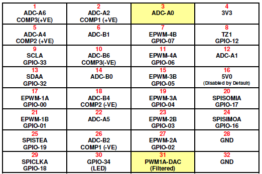
Moram da napomenem da je PWM na pinu 31 filtriran low pass filterom, tako da umesto četvrtki koje generiše PWM na osciloskopu vidimo adekvatan napon, ali samo pod uslovom da je frekvencija nosioca dovoljno velika.
Zadaci
Zadatak 1
Napraviti program u CSS-u koji će uz pomoć hardverskog PWM-a DSP-a (PWM1A) generisati jednosmeran napov od 2V.
Korišćenjem osciloskopa proveriti vrednost generisanog napona.
Rešenje
#include "PeripheralHeaderIncludes.h"
#include "DSP2802x_EPwm_defines.h"         // useful defines for initialization

void DeviceInit(void);
void InitFlash();
void MemCopy(Uint16 *SourceAddr, Uint16* SourceEndAddr, Uint16* DestAddr);

// Used for running BackGround in flash and the ISR in RAM
extern Uint16 RamfuncsLoadStart, RamfuncsLoadEnd, RamfuncsRunStart;

void initPWM(long period, long duty_cycle) {
  // Time-base registers
    EPwm1Regs.TBPRD = period;              // Set timer period, PWM frequency = 1 / period
    EPwm1Regs.TBPHS.all = 0;               // Time-Base Phase Register
    EPwm1Regs.TBCTR = 0;                       // Time-Base Counter Register
    EPwm1Regs.TBCTL.bit.PRDLD = TB_IMMEDIATE;  // Set Immediate load
    EPwm1Regs.TBCTL.bit.CTRMODE = TB_COUNT_UP; // Count-up mode: used for asymmetric PWM
    EPwm1Regs.TBCTL.bit.PHSEN = TB_DISABLE;       // Disable phase loading
    EPwm1Regs.TBCTL.bit.SYNCOSEL = TB_SYNC_DISABLE;
    EPwm1Regs.TBCTL.bit.HSPCLKDIV = TB_DIV1;
    EPwm1Regs.TBCTL.bit.CLKDIV = TB_DIV1;

    // Setup shadow register load on ZERO
    EPwm1Regs.CMPCTL.bit.SHDWAMODE = CC_SHADOW;
    EPwm1Regs.CMPCTL.bit.LOADAMODE = CC_CTR_ZERO; // Load on CTR=Zero

    // Set compare values
    EPwm1Regs.CMPA.half.CMPA = duty_cycle;          // Set duty 50% initially

    // Set actions
    EPwm1Regs.AQCTLA.bit.ZRO = AQ_SET;            // Set PWM1A on Zero event
    EPwm1Regs.AQCTLA.bit.CAU = AQ_CLEAR;          // Clear PWM1A on Up-Count CompareA event
}

void updateDutyCycle (long duty_cycle) {
    EPwm1Regs.CMPA.half.CMPA = duty_cycle;
    // Update the duty cycle and hence voltage
    // level of the PWM1A_DAC output (the value
    // must be between 0 and period)
}

void initADC() {
    Uint16 i;

    EALLOW;
    AdcRegs.ADCCTL1.bit.ADCREFSEL   = 0;     // use internal band gap reference
    AdcRegs.ADCCTL1.bit.ADCBGPWD    = 1;    // power up band gap
    AdcRegs.ADCCTL1.bit.ADCREFPWD    = 1;    // power up reference
    AdcRegs.ADCCTL1.bit.ADCPWDN     = 1;    // power up rest of ADC
    AdcRegs.ADCCTL1.bit.ADCENABLE    = 1;    // enable ADC output
    for(i=0; i<5000; i++){}                    // wait 60000 cycles = 1ms (each iteration is 12 cycles)

    AdcRegs.ADCCTL1.bit.INTPULSEPOS    = 1;    // create int pulses 1 cycle prior to output latch

    //EOC = end of conversion event, SOC = start of conversion event
    AdcRegs.INTSEL1N2.bit.INT1SEL = 0;        // ADCCH0 (ADC-A0) EOC causes ADCInterrupt1
    AdcRegs.INTSEL1N2.bit.INT1CONT = 1;        // set ADCInterrupt 1 to auto clr (continuous conversion)
    AdcRegs.INTSEL1N2.bit.INT1E = 1;        // enable ADCInterrupt1; 0=none, 1=ADCInt1, 2=ADCInt2

    AdcRegs.ADCINTSOCSEL1.bit.SOC0 = 1;        // ADCInterrupt1 causes SOC0
    AdcRegs.ADCSOC0CTL.bit.CHSEL= 0;         // convert ADC-A0 (CH0) when SOC0 is received
    AdcRegs.ADCSOC0CTL.bit.ACQPS = 6;        // set S/H window to 6 clk cycles (117ns)

    AdcRegs.ADCSOCFRC1.all = 0x0001;          // kick start ADC by causing an ADCInterrupt1 event
    EDIS;
}

Uint16 readADC() {
    return AdcResult.ADCRESULT0;
}

void main() {
    // Inicijalizuj DSP
    DeviceInit();    // Device Life support & GPIO mux settings
#ifdef FLASH
    MemCopy(&RamfuncsLoadStart, &RamfuncsLoadEnd, &RamfuncsRunStart);
    InitFlash();    // Call the flash wrapper init function
#endif //(FLASH)

    // Inicijalizuj PWM
    Uint16 period = 60;  // 1MHz when PLL is set to 0xC (60MHz); 60MHz / 60 = 1MHz
    float vcc = 3.3;
    float napon = 2; // Trazeni napon iz Zadatka 1
    Uint16 duty_cycle = (napon/vcc)*period;
    initPWM(period, duty_cycle);

    while(1) {
    }
}
U primeru se nalaze funkcija za inicijalizaciju ADC i uzimanje vrednosti sa ADC-a, što za ovaj zadatak nije naročito bitno, ali za sledeće će biti.
Zadatak 2
Napraviti program koji generiše signale:
- sinusoide učestanosti 600Hz,
- četvrtki učestanosti 150Hz,
- trougla učestanosti 300Hz i
- rampe učestanosti 300Hz.
Sve signale aproksimirati sa 50 odbiraka i izbaciti na PWM1A. Amplituda signala treba da bude maksimalna moguća, a učestanost nosioca PWM-a postaviti na 1MHz. Koristeći ADC razvojnog sistema proveriti da li su signali ispravno generisani.
Signal generisati uz pomoć lookup tabela (PDSPlib) ili IQMath biblioteke.
Rešenje
void podesiTajmer(long i) {
    if (i>0) {
        CpuTimer0Regs.PRD.all = i;  // Setujem tajmer na i broj otkucaja kloka
        CpuTimer0Regs.TCR.bit.TRB = 1;  // Resetujem Timer (Timer Reload Bit)
        CpuTimer0Regs.TCR.bit.TIF = 1;  // Resetujem TIF
    }
}

void cekajDaIstekneTajmer() {
    // Kada istekne vreme postavljeno u PRD (Period) registar dogodice se prekid tajmera
    // Da se prekid desio mozemo videti posmatrajuci TIF (Timer Interrupt Flag),
    // Koji ce se u trenutku prekida postaviti na 1.
    while(!CpuTimer0Regs.TCR.bit.TIF);  // Cekam da istekne tajmer, odnosno da se desi interrupt
    CpuTimer0Regs.TCR.bit.TIF = 1;  // Resetujem TIF
}

Uint16 izlaz[50];
void main() {

    // Inicijalizuj DSP
    DeviceInit();    // Device Life support & GPIO mux settings
#ifdef FLASH
    MemCopy(&RamfuncsLoadStart, &RamfuncsLoadEnd, &RamfuncsRunStart);
    InitFlash();    // Call the flash wrapper init function
#endif //(FLASH)

    // Inicijalizuj PWM
    Uint16 period = 60;  // 1MHz when PLL is set to 0xC (60MHz); 60MHz / 60 = 1MHz

    // Zadatak 1
    float vcc = 3.3;
    float napon = 1.5; // Trazeni napon iz Zadatka 1
    Uint16 duty_cycle = (napon/vcc)*period;

    initPWM(period, duty_cycle);

    // Inicijalizuj ADC
    initADC();

    // Zadatak 2 - sinusoida
    Uint16 i;
    long duty;
    long brOdbiraka = 50;
    _iq korak = _IQ(6.28)/brOdbiraka;

    podesiTajmer(2000); // 600Hz
    while(1) {
        for (i=0; i<brOdbiraka; i++) {
            duty_cycle=period*_IQtoF(_IQsin(i*korak)+_IQ(1))/2;
            updateDutyCycle(duty_cycle);
            cekajDaIstekneTajmer();
            izlaz[i]=readADC();
        }
    }
}
Rešenje sa primera je samo za generisanje sinusoide. Da bi ovaj kod radio, u zadatku 1 je potrebno zameniti main() i dodati funkcije podesiTajmer() i cekajDaIstekneTajmer().
Zadatak 3*
Napraviti program koji generiše signal sastavljen od zbira sinusoida učestanosti 600Hz i 900Hz, maksimalnih amplituda. Signal treba da bude zašumljen šumom amplitude 5% od maksimalne. Signal aproksimirati sa željenim brojem odbiraka i poslati ga na PWM čija učestanost nosioca treba da bude 1MHz. Koristeći ADC razvojnog sistema proveriti da li je signal ispravno generisan.